
 VI
VI JP
JP 中文 (台灣)


Chip-mounting technique in SMT surface packaging technology
Different brands own different know-how and exclusive technology. They are different when making different types of chips mounted on SMT lines. However, the stages from loading to finished products are quite similar. The stages include: 1) Scan the solder alloy (solder paste) onto the bare board. 2) Mount the IC and the IC. 3) Heating – cooling. 4) Check and correct errors.Scan alloy welding
On non-perforated printed circuit surfaces, conductive layers of conductive materials such as tin-lead, silver or gold are plated. These details are called solder pins. Then, the solder paste in the form of a paste is a mixture of solder alloys and welding material particles. They are scanned onto the surface of printed circuit board. People use a special device, such as metal masks (or stencil), to prevent solder paste from getting on unwanted places. They are made of thin stainless steel film. On it is processed the position corresponding to where the chip is located on the board. In this way, solder paste will be scanned into the desired position. Another method is to attach the device to the other side of the board. It is the use of a numerical control device to place dots of highly adhesive material in the position of the component. The final stage is when solder paste is coated on the surface. At this point, the motherboard will be transferred to a pick-and-place machine.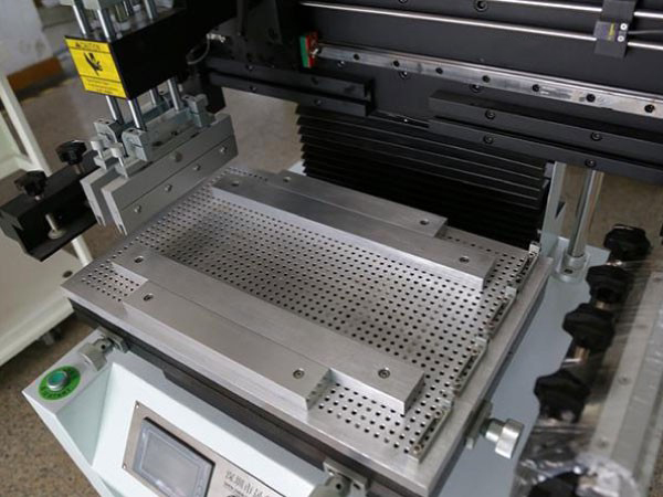
Mount the IC, attach the IC
Small sized SMDs are usually conveyed to the transmission line on the tape. They will revolve around a certain axis. Meanwhile IC is usually stored in separate trays. The numerically controlled chip picker will remove the chips from the tray. Next place them on the PCB surface where the solder paste is scanned. Components on the underside of the board are mounted first. The glue spots are then quickly dried by heat or by UV radiation. The board was then flipped over and the device attached to the motherboard finished the rest of the board.
Heating – cooling
After the process of attaching the components is completed, the board will be transferred to the oven. The boards first entered the preheating zone. Here the temperature of the board and all the components are relatively uniform. They will be raised slowly. This minimizes thermal stress when the assembly process is finished after welding. The board then enters the area with a temperature high enough to melt molten particles in solder paste. Next it will solder the components on the board. The surface tension of molten solder paste prevents components from dislocating. If the geographical surface of the welding leg was fabricated as designed. The surface tension will automatically adjust the component to its correct position.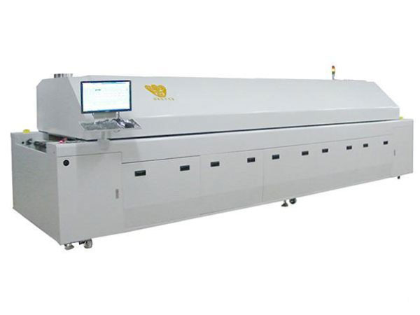 There are many techniques used for heating and tempering of the board after the process of picking and attaching. Such techniques as using infrared light, hot air. In special cases one can use CF4 liquid with a large number of heat. This technique is called gia. Nitrogen or nitrogen-rich compressed air is currently used in convection ovens. Of course, each method has its advantages and disadvantages.
First with the annealing method using IR. Engineers must arrange components on the lower board that do not fall into the area of higher components. It is easy if the designer knows about heat cycles or convection welding in advance. For some designs, manual welding or assembly of special components is required. Or further automate using centralized infrared devices.
After welding, the boards must be “washed” to remove the soldering material on them. Different welding materials are washed with different chemicals and solvents. The remainder is dissolved solvent which is washed with clean water. They will be quickly dried with compressed air.
There are many techniques used for heating and tempering of the board after the process of picking and attaching. Such techniques as using infrared light, hot air. In special cases one can use CF4 liquid with a large number of heat. This technique is called gia. Nitrogen or nitrogen-rich compressed air is currently used in convection ovens. Of course, each method has its advantages and disadvantages.
First with the annealing method using IR. Engineers must arrange components on the lower board that do not fall into the area of higher components. It is easy if the designer knows about heat cycles or convection welding in advance. For some designs, manual welding or assembly of special components is required. Or further automate using centralized infrared devices.
After welding, the boards must be “washed” to remove the soldering material on them. Different welding materials are washed with different chemicals and solvents. The remainder is dissolved solvent which is washed with clean water. They will be quickly dried with compressed air.
Check and correct errors
The board is taken to the optical inspection department to detect errors. In case of necessity, we can install a number of optical inspection stations for the technological lines.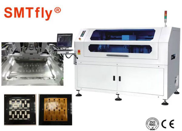 At this stage we can use optical AOI (Automated Optical Inspection) or use X-ray. These devices detect the position errors, contact errors of components and solder paste on the surface of the printed circuit.